In March 2026, HBM4 mass production has officially arrived. Discover how 16-layer stacking and HCB technology are breaking the memory wall for NVIDIA’s Vera Rubin and next-gen on-device AI.
The 2048-Bit Revolution: Shattering the Memory Wall
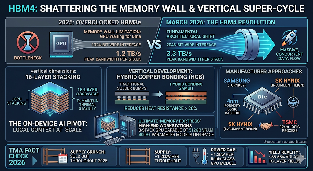
By March 2026, the semiconductor industry has officially moved past the “overclocked” limitations of HBM3e. The HBM4 standard has arrived with a literal structural expansion: a 2048-bit wide memory interface. This doubles the bus width of previous generations, enabling a peak bandwidth of 3.3 TB/s per stack.
This isn’t just a spec bump; it’s a fundamental architectural shift. While 2025-grade AI accelerators struggled with the “Memory Wall”—where GPUs spent more time waiting for data than processing it—HBM4 allows for the massive, concurrent data flows required by [Autonomous Digital Workers]. For NVIDIA’s Vera Rubin platform, HBM4 is the oxygen that allows its massive tensor cores to breathe.
16-Layer Stacking and the Hybrid Bonding Gambit
The real “Yield War” of 2026 is being fought in the vertical dimension. We have moved from 12-layer to 16-layer stacks, pushing single-stack capacities to 48GB and 64GB.
To achieve this without the chip becoming a thermal meltdown, manufacturers are abandoning traditional solder bumps for Hybrid Copper Bonding (HCB).
- Samsung has taken a “Turnkey” approach, leveraging its 4nm foundry to build its own logic base dies.
- SK Hynix, the reigning incumbent, has solidified its alliance with TSMC, using the latter’s 12nm logic process to serve as the “brain” of its HBM4 stacks.
This transition to HCB reduces heat resistance by over 20%, allowing 16-layer devices to maintain stable performance under the brutal workloads of 2026-class inference.
The On-Device AI Pivot: Local Context at Scale
While data centers are the primary consumers, HBM4 is beginning to trickle down into high-end workstations. As discussed in [The On-Device AI Mirage], memory bandwidth was the primary bottleneck for local LLMs. HBM4 changes the TCO of “Private AI.”
With an 8-stack GPU configuration now capable of holding 512GB of VRAM, the need to shard models across multiple machines is disappearing. In March 2026, we are seeing the first workstations capable of running 400B+ parameter models entirely on-device, providing the ultimate “Memory Fortress” for corporations obsessed with data sovereignty.
“The February production launch of HBM4 marks the beginning of a new era, not the end of supply constraints. Allocation battles between hyperscalers will define the 2026 fiscal year.” — TMA Memory Analyst, March 2026.
TMA Fact Check 2026
- The Supply Crunch: SK Hynix has officially “sold out” its entire 2026 HBM4 production capacity as of this month. Micron and Samsung are reporting similar backlog levels, with delivery windows for non-hyperscale buyers stretching into late 2027.
- The Power Gap: Despite a 40% improvement in energy efficiency per bit, HBM4’s massive bandwidth means total power draw for a Rubin-class GPU module is still projected to exceed 1.2kW, necessitating the [Submerged Edge] liquid cooling solutions we previously analyzed.
- The Yield Reality: 16-layer HBM4 yields remain a guarded secret, but industry whispers suggest a volatile 55-65% range, significantly lower than the mature HBM3e lines, keeping prices at historic highs through H2 2026.
Related Deep Analysis
- [The On-Device AI Mirage: Why Your 2026 PC Is a Local LLM Prison]
- [Beyond Blackwell: NVIDIA GTC 2026 and the Birth of the Vera Rubin AI Factory]
- [The Submerged Edge: Why Immersion Cooling is the Silent Pulse of 2026 AI]
The Sharp Question
As memory becomes a “Strategic Weapon” controlled by just three companies, are we entering a period of “Silicon Rentierism,” where the cost of intelligence is permanently high because we’ve reached the physical limits of how many layers of silicon we can stack before they break?
#HBM4 #SK Hynix #Samsung #NVIDIA Vera Rubin #16-layer Stacking #Hybrid Bonding #AI Memory #Tech Macro