The biting March wind from the Han River seeps through the studio window this morning, a reminder that the physical world always finds a way to chill even the most heated tech hype. I’m sitting here in Gimpo, staring at the schematic of a 2nm wafer. My fingers trace the cold, metallic surface of my desk as I realize the industry has been staring at the wrong side of the silicon for thirty years.
A deep dive into Backside Power Delivery Network (BSPDN) technology. Analyze how Samsung, TSMC, and Intel are using 2nm “backdoor” engineering to break the IR drop barrier in 2026.
Abandoning the Front Yard: The Geometry of Desperation
For three decades, we crammed data lines and power lines onto the front of the wafer like commuters on a Seoul subway at rush hour. But as we hit the 2nm threshold, this “cohabitation” became a catastrophe. “Wiring Congestion” and “IR Drop” (voltage sag) have become the ghost in the machine, choking performance just as the world demands infinite compute for Agentic AI.
Enter BSPDN (Backside Power Delivery Network). The concept is deceptively simple: leave the data on the front, and move the power to the back. Intel called it ‘PowerVia’ and struck first. Now, Samsung and TSMC are betting their 2nm survival on this “backdoor” maneuver. By utilizing the backside of the wafer, power efficiency jumps by over 30%, and chip area shrinks by 15%. This isn’t just an upgrade; it’s a surgical relocation of the chip’s entire vascular system.
The 2nm Siege: Attacking TSMC’s Fortress from Behind
From my perspective as a veteran critic, BSPDN is the sharpest blade available to those looking to cut into TSMC’s dominant market share. While TSMC has the luxury of caution, Intel is sprinting to deploy this tech to reclaim its lost throne. Samsung, meanwhile, is betting on “Next-Gen 2nm” yields to restore its tarnished technical leadership.
This shift isn’t occurring in a vacuum. It aligns perfectly with the Mexico’s Ascent as a Strategic Weapon that we’ve discussed previously. High-value 2nm chips require extreme bonding precision and warpage control. The fabs that master BSPDN will be the ones chosen to anchor the “Intelligent Manufacturing” hubs in North America and beyond. If you can’t manage the heat and the power from the back, you don’t belong in the 2026 vanguard.
“TSMC’s walls look impenetrable from the front, but the ‘back door’ of BSPDN is wide open for anyone brave enough to master the yield. The foundry war is no longer about who can draw the smallest line, but who can engineer the most efficient vein.” — TMA Senior Editor
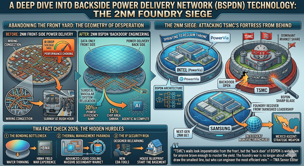
TMA Fact Check 2026: The Hidden Hurdles
- The Bonding Bottleneck: BSPDN requires thinning the wafer to an extreme degree and then bonding it with surgical precision. One micron of deviation, and the entire batch is scrap. This is where the HBM4 Yield War experience becomes a prerequisite.
- Thermal Management Paranoia: Moving power to the back changes the entire heat profile of the chip. Standard cooling solutions are being rendered obsolete overnight, creating a massive secondary market for advanced liquid cooling.
- The IP Security Risk: Backside delivery requires new EDA (Electronic Design Automation) tools. Designers are essentially relearning how to build a house by starting with the plumbing in the basement.
Related Deep Analysis
- The HBM4 Yield War: SK Hynix’s Lead vs. Samsung’s Desperate ‘All-In’ Gamble
- Mexico’s Ascent as a Strategic Weapon in the AI Yield War
- The 2026 Resilience Report: How to Survive the 6G Era
The Sharp Question
Are you still obsessed with the “nanometer” number on the box, or have you recognized that the real revolution is happening where no one can see it—on the back of the wafer? In 2026, if you aren’t looking at the flip side, you’re looking at the past.
#2nm Process #BSPDN #PowerVia #Foundry War #TSMC #Samsung Electronics #Intel #Semiconductor Strategy