A light haze of spring dust clings to the studio window in Nusan-ri this morning, diffusing the sharp April sun into a muted, clinical glow that mirrors the very circuitry I’m currently deconstructing. The silence here is absolute, broken only by the low, industrial hum of my laptop and the rhythmic, metallic clink of a spoon against my mug.
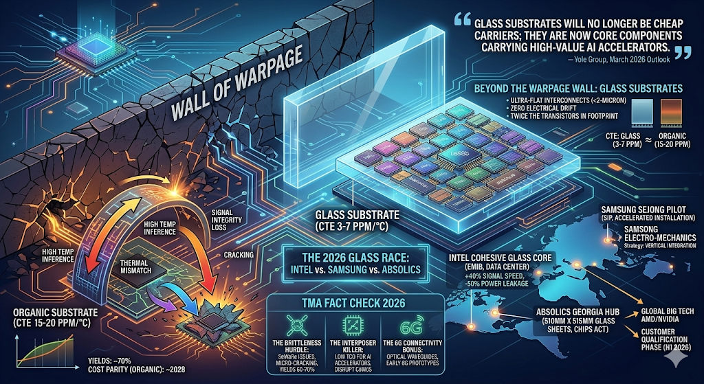
The prose I’ve spent the morning sharpening—bitter and dry as the espresso in my hand—stands in stark contrast to the brittle, transparent future currently being forged in the cleanrooms of Intel and Samsung. We are witnessing the twilight of the organic resin era. The “Warpage Wall” has been hit, and the industry is now shattering its legacy foundations to rebuild on a substrate of glass.
The semiconductor industry hits the “Warpage Wall” in 2026. Discover how Intel, Samsung, and Absolics are pivoting to glass substrates to power the next generation of AI super-packages.
The Warpage Wall: Why Organic Materials Failed
For thirty years, organic resin-based substrates (like ABF) were the silent workhorses of the industry. But as we entered 2026, the demand for “Super-Packages”—monstrous arrays combining logic dies with HBM3e/4 memory—pushed these materials to their physical limit. Organic substrates expand and contract at rates vastly different from silicon, leading to the dreaded “Warpage Wall.” At the high temperatures required for AI inference, traditional substrates bow and crack, destroying signal integrity.
Glass changes the fundamental math of the package. Its Coefficient of Thermal Expansion (CTE) is nearly identical to silicon (3-7 ppm/°C). This allows for ultra-flat surfaces that can support sub-2-micron interconnects. In plain English: glass doesn’t move when it gets hot, allowing us to cram twice as many transistors into the same footprint without the risk of electrical drift.
The 2026 Leaders: Intel and Samsung’s Pilot Dominance
By March 2026, the “Glass Race” has a clear front-runner. Intel has officially integrated “Thick-Core” glass substrates with its EMIB (Embedded Multi-die Interconnect Bridge) technology, aiming at the data center market. Intel’s internal data suggests that glass-core processors can deliver up to 40% better signal speed while effectively cutting power leakage in half.
Samsung Electro-Mechanics is not far behind. Having accelerated its equipment installation in Sejong, South Korea, Samsung is now producing pilot products for high-end System-in-Package (SiP) applications. Their strategy is a vertical integration play, combining Samsung Display’s glass processing expertise with Samsung Electronics’ foundry capabilities.
Absolics and the Georgia Manufacturing Hub
The geopolitical dimension of this shift is centered in Covington, Georgia. Absolics, a subsidiary of SKC, has officially entered the customer qualification phase in H1 2026. Backed by $75 million in CHIPS Act funding, the facility is producing mass-production samples for “Global Big Tech”—widely understood to include AMD and NVIDIA.
The appeal of Absolics’ glass panels lies in scale. By using large 510mm x 515mm glass sheets rather than traditional round wafers, they are targeting a yield advantage that could eventually bring glass-to-organic cost parity by 2028.
“Glass substrates will no longer be cheap carriers; they are now core components carrying high-value AI accelerators. 2026 is the node where glass enters commercial shipments.” — Yole Group, March 2026 Outlook.
TMA Fact Check 2026
- The Brittleness Hurdle: While glass is thermally superior, it is mechanically brittle. The industry is currently struggling with “SeWaRe” (Substrate-level Warpage and Reliability) issues, specifically micro-cracking during the dicing process. Yields for large-format glass substrates are currently hovering between 60-70%, far below the 90%+ seen in mature organic lines.
- The Interposer Killer: Glass substrates can act as their own interposers. This could potentially disrupt the market for TSMC’s CoWoS (Chip on Wafer on Substrate) by removing the need for separate silicon interposers, significantly lowering the Total Cost of Ownership (TCO) for AI accelerators.
- The 6G Connectivity Bonus: Beyond AI, the transparency of glass at specific wavelengths allows for the embedding of optical waveguides directly into the substrate, making it a critical material for the first 6G networking prototypes emerging in late 2026.
The Sharp Question
If glass substrates successfully eliminate the silicon interposer, we are looking at a massive power shift away from traditional foundries toward specialized material giants. Are we ready for a supply chain where a shortage of high-purity glass becomes as catastrophic as the 2021 chip drought?
#Glass Substrate #Advanced Packaging #Intel #Samsung #Absolics #AI Accelerators #Semiconductor Macro